Background
The 24LC256 is an I2C-based EEPROM IC.
We will create a generic I2C driver which will then be layered with 24LC256-specific API’s.
The main learning is performing read/write operations on external memory.
As always, I’ll discuss the theory then wrap it up with a practical component.
The Theory
Introducing the 25LC256 EEPROM IC
Unlike RAM, EEPROM is non-volatile.
Flash memory is EEPROM but better. It’s significantly cheaper and has faster write times.
This project uses the 25LC256. It can store 32kB of memory. As a reference, the ATmega328p as 32kB of flash. Thus, by using this we’re doubling our memory.
If we sample a temperature sensor every 5 minutes, with 32kB we can store 3 months of data.
The 25LC256 IC has 6 commands
- Read
- Write
- Write-enable
- Write-disable
- Read status
- Write status
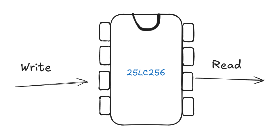
To perform a read, you:
- Send read command
- Specify memory start address
- Keeping clocking SCK until you get you’re data. The data keeps getting shifted out
To perform a write, you:
- Send write-enable command
- Send write command
- “Write in” your data, upto 64 bytes or a page
- Set SS HIGH
I mentioned a page. This is how the memory is arranged in the 25LC256. Into chunks of 64 bytes. This is called a page of memory. It’s used to accelerate write times. A single write operation is slow, taking 5ms. However, writing a page of memory also takes 5ms. Thus, if you’re smart write pages of memory, it will be 64x faster!
Also, since write operations are slow, the IC has a status bit indicating when the write operation has finished.
Capacity
The 24LC256 stores 32 KB (32,768 bytes) of non-volatile data — the same amount as the ATmega328P’s entire flash program memory. Connecting one effectively doubles the total memory available to the system.
To make that concrete: if you log a temperature reading every 5 minutes, one byte per reading, 32 KB gives you:
32,768 bytes ÷ (288 readings/day) ≈ 113 days (~3.7 months) of dataThe chip retains data without power for over 200 years and survives more than 1,000,000 write cycles per address (24LC256 datasheet p. 3).
Two Fundamental Operations
The SPI cousin of this chip (the 25LC256) has 6 explicit opcodes: READ, WRITE, WREN (write-enable), WRDI (write-disable), RDSR (read status), and WRSR (write status). Each operation starts by sending one of these command bytes over SPI.
The I2C 24LC256 reduces this to 2 operations — read and write — because I2C encodes direction differently:
- Write — the master holds the R/W bit low in the device address byte, sends the memory address, then clocks out data bytes.
- Read — the master first sends a write-address frame (a “dummy write”) to set the chip’s internal address pointer, then issues a Repeated START with the R/W bit high to switch bus direction and clock in data.
There is no WREN opcode. Write protection is handled entirely by the hardware WP pin: tie it low (GND) to allow writes; tie it high (VCC) to make the array read-only.
There is no status-register opcode either. The chip signals that a write cycle is still in progress by NACKing any attempt to address it on the bus — a technique the datasheet calls acknowledge polling (p. 6). This driver takes the simpler approach of waiting a fixed 5 ms after every STOP.
Pages
The 24LC256’s memory is organised into 512 pages of 64 bytes each (512 × 64 = 32,768 bytes).
This matters for write speed. A single byte write and a 64-byte page write both take the same internal write cycle time: Twc = 5 ms maximum. Writing byte-by-byte therefore wastes 63/64 of the available throughput:
| Strategy | Bytes written | Write cycles | Time |
|---|---|---|---|
| Byte-by-byte | 32,768 | 32,768 | ~164 s |
| Page writes (64 B) | 32,768 | 512 | ~2.6 s |
EEPROM_clear_all() exploits this by filling 64 bytes per I2C transaction, achieving the 64× speedup. The constraint: all bytes in a page write must fall within the same aligned 64-byte page (address bits A5..A0 are an internal page counter that wraps at the boundary, not an incrementing address). Crossing a page boundary silently overwrites bytes at the start of the same page.
Project 1 – The “Hello World” project
Hardware Connections
Since the 25LC256 is 5V compatible, that simplifies the design. The schematic is available in the GitHub repository.
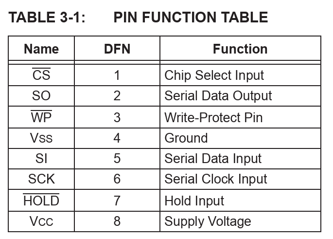
- A 1k pullup on CS ensures that the CS is HIGH, avoiding a possibility of the IC interfering when performing ICSP.
- The 25LC256 transmits data on pin 2 (Serial Output). This connects to MISO, since the master will be IN’ing the data as the slave OUT’s the data.
- Also, for simplicity, we’ll connect pin 3 (CS), and pin 7 (HOLD) to Vcc. We won’t restrict write operations.
The Software
The project consists of various files:
- An I2C generic driver (.c/.h file)
- The 25LC256 driver (.c/.h file)
main.c
As always, full source code is available in my GitHub repository.
main.c prints first 10 bytes in the first 10 memory address locations. Afterwards, a UI appears, presenting the user with 2 actions they can take to interact with the IC. E to erase all memory or w to write a byte to memory.
After an instruction finishes, the first 10 bytes of memory are displayed (since it’s in the while loop).