Background
Often there is a mandatory requirement to power microcontrollers and components from either 5V or 3.3V.
In my experience, the bottleneck is transferring a prototype to a product is to make it battery-powered.
Also, there’s nothing worse than developing a project and realizing it can’t leave your computer since it’s powered either by USB or a wall-wart.
These requirements form the motivation for this project. Hazard can be integrated as part of a larger project if you like. This is my approach to projects. To build small, modular systems that like LEGO you can connect to form more advanced systems. This system makes any project battery-powered. Nothing else.
Introduction to Battery Charging
Unlike LiPo batteries, Lithium-Ion cells do not ship with built-in protection circuitry. When you buy raw cells (most commonly the 18650), everything around them — charge control, protection, and safe voltage and current limits — is up to the designer. Therefore, there is a requirement for dedicated charging circuitry to safely bring the cell from empty to full without damaging the cell or the surrounding electronics.
Battery chargers generally use one of two topologies: linear or switched-mode. This is similar to the two types of DC-DC conversion: Linear and switched-mode.
Linear chargers drop the input voltage to the battery voltage through a pass FET. The majority of the heat and power dissipation occurs in this component, as it single-handedly burning off the excess voltage as heat. This makes linear chargers simple and cheap, but inefficient — especially when the dropout voltage increases.
A switched-mode charger, by contrast, uses an inductor and two FETs to transfer energy in pulses rather than dissipate it. The premise is we use the inductor as an energy-storage element.
Requirements of a Battery Charger
A proper battery charger should provide charging detection, short-circuit detection, over-current detection, undervoltage-lockout (UVLO), and reverse-polarity protection. The TP4056 fulfils most of these requirements — charge detection, current regulation, and UVLO among them.
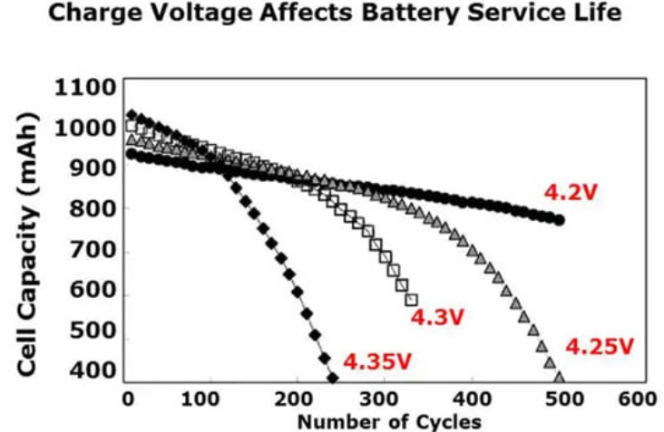
In order to extend the lifespan of a Li-Ion battery it is paramount to supervise the charging process. The graph below conveys the dangers of overcharging. Increasing the cell voltage by 0.1V, approximately halves the lifespan. Additionally, charging the battery too rapidly, results in cell degradation. Thus, it is pivotal to adopt excellent charge circuitry
Customer Requirements and Engineering Specifications (CRES)
This table conveys the product features and the design requirements. It protects against feature-creep.
| Category | ID | Engineering Specification | Justification |
|---|---|---|---|
| Power & Output | #1 | Provide a user-selectable regulated output of 3.3 V or 5 V via an onboard switch. | Supporting both common logic rails lets Hazard power a wide range of MCUs, sensors and modules without an external regulator. |
| Power & Output | #2 | Boost the single 18650 cell (2.5–4.2 V) up to a stable 5 V rail using the onboard boost converter (U2). | A boost stage delivers a consistent USB-level 5 V regardless of the cell’s state of charge. |
| Power & Output | #3 | Maintain output regulation across the full battery discharge range. | Downstream devices must see a stable rail from a full to a nearly depleted cell. |
| Charging | #4 | Recharge the battery through a USB 2.0 Type-A receptacle. | USB-A cables and chargers are ubiquitous, so no dedicated adapter is required to recharge Hazard. |
| Charging | #5 | Manage Li-ion charging on-board (TP4056-class, ~500 mA CC/CV charge current). | Provides safe constant-current / constant-voltage charging of the 18650 cell; ~500 mA verified during testing. |
| Charging | #6 | Include a series Schottky / reverse-polarity protection diode on the USB input. | Protects against incorrect connection and lowers charge-IC heat dissipation. |
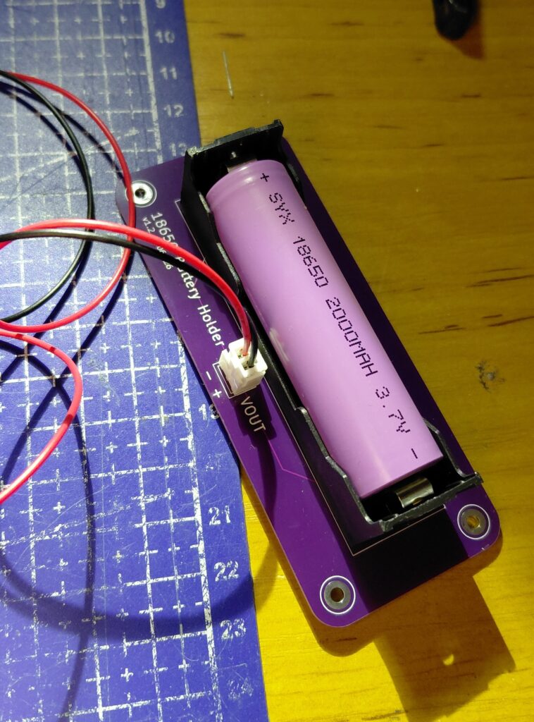
| Battery | #7 | Use a rechargeable, swappable 18650 Li-ion cell on a dedicated holder board. | Decoupling the cell from the main board keeps it battery-agnostic and supports swappable cells via a standard interface. |
| Interface & Connectors | #8 | Link the battery-holder board and power board using 2-pin JST-XH connectors for VBAT and VOUT. | Keeps the two boards mechanically and electrically separable with a keyed, reliable connector. |
| Interface & Connectors | #9 | Provide a power switch with an output indicator LED. | Lets the user enable/disable the boost output and confirm at a glance that the rail is live. |
| Validation & Test | #10 | Expose test pads for key nets (VBUS, VBAT, VOUT, GND). | Enables quick multimeter probing during bring-up and troubleshooting. |
| Mechanical Design | #11 | Provide mounting holes on both PCBs. | Allows secure fixturing / enclosure mounting and mechanical strain relief. |
| Mechanical Design | #12 | Adopt a two-board architecture: a separate battery-holder PCB and the power PCB. | Simplifies cell replacement and reuse while keeping the main board battery-agnostic. |
| Mechanical Design | #13 | Keep a compact PCB footprint (~88 × 22 mm guide) with rounded corners. | Keeps the pack pocketable and improves handling and aesthetics. |
| Cost & Documentation | #14 | Minimise BOM cost using JLCPCB standard-library, E-series component values. | Avoids per-part extended-component fees and uses commonly available values. |
| Cost & Documentation | #15 | Source all ICs with datasheets from reputable manufacturers. | Ensures reliable specifications and design references for the build. |
The Theory
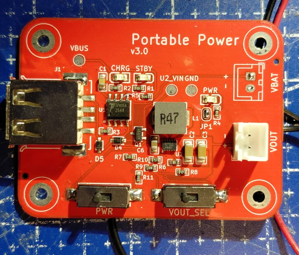
We’ll use a lithium ion battery of any capacity. We’ll connect it to a TP4056 so we can charge it when it depletes during use. We’ll connect that to a TPS63802 to boost it to 5V or 3.3V since the voltage of the lithium ion battery can vary from 2.7V to 4.2V.
The lithium ion battery can be charged via USB 2.0 receptacle.
Introducing the TP4056
Overview
The TP4056 is a 1A linear CC/CV single-cell Li-Ion battery charger designed to run from USB power, which is convenient given how ubiquitous USB sources are — power banks, laptops, or wall warts. Being a linear charger makes it simple, low-cost, and compact on the PCB, at the cost of lower efficiency and higher power dissipation compared to switching alternatives.
Key Features
- Programmable charge current up to 1A
- Fixed 4.2V float voltage
- Undervoltage lockout (UVLO)
- Integrated soft-start (no
SSpin required) - Internal die temperature regulation at 145°C
- Shutdown sleep mode via the
CEpin (supply current drops to 55µA)
Pin Functions
TEMP (Pin 1) — Connects to the battery’s NTC thermistor. Charging is suspended if V_TEMP exceeds preset thresholds.
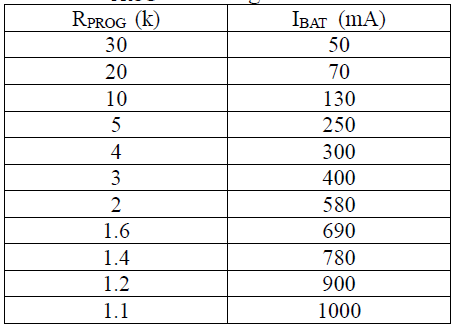
PROG (Pin 2) — Sets the charge current via an external resistor: R_PROG = 1100 / I_BAT
STDBY (Pin 6) — Pulled LOW when a charge cycle completes. Connecting a green LED between VCC and this pin makes it illuminate to indicate that charging has completed.
CHRG (Pin 7) — Pulled LOW while the battery is charging. Connecting a red LED between VCC and this pin makes it illuminate during an active charge cycle.
Both STDBY and CHRG are open-drain outputs. This means the drain terminal of an internal FET is exposed directly on the pin.
Understanding the active-low signalling. STDBY and CHRG are open-drain outputs. When the datasheet says the pin is pulled LOW under certain conditions, it means the internal FET begins conducting and sinks the pin to GND. The LOW level at the pin is the result of the FET turning on, not its cause. This is what “active-low” means: the pin’s asserted state is LOW. The TP4056 then sinks the current flowing through the external LED, illuminating it. So although we usually associate a LOW signal with something being off, here it means the opposite — the IC is actively sinking current, which is the whole point of open-drain signalling.
CE (Pin 8) — Chip Enable. When tied HIGH (to VCC), the TP4056 operates normally; otherwise it enters shutdown mode. Can be driven from a microcontroller I/O to minimise power consumption. If VCC < V_BAT or VCC is disconnected, the TP4056 also enters shutdown mode, and the battery drain current drops to 3µA.
Charge Cycle Operation
As the battery charges from 2.4V to 4.2V, it passes through three stages:
- Pre-charge (Trickle) — for deeply discharged cells
- Fast charge (Constant Current, CC)
- Taper (Constant Voltage, CV)
A charge cycle begins once all of the following are true:
- VCC is above the UVLO threshold
- A program resistor is connected to
PROG CEis HIGH
To signal the start of the cycle, CHRG is pulled LOW.
If the battery voltage is below 3V, the TP4056 enters trickle-charge mode, gently raising V_BAT to a safe level for full-current charging. Once V_BAT exceeds 3V, it transitions into fast-charge CC mode, ramping the current up to the value set by R_PROG.
When V_BAT reaches the 4.2V float voltage, the TP4056 switches to CV mode. The current then tapers off, and once it drops to 1/10 of the programmed current, the charge cycle ends. STDBY is pulled LOW to signal completion, and the TP4056 enters standby mode, dropping the input supply current to 55µA.
A new charge cycle is automatically initiated if V_BAT falls below 4.05V.
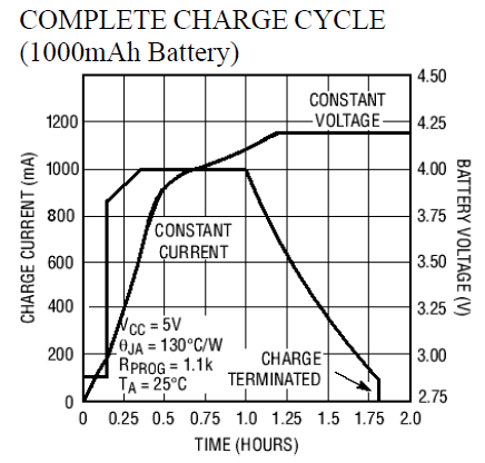
The charge cycle can be interrupted at any time by pulling CE LOW, which forces the TP4056 into shutdown mode — dropping I_BAT to 2µA and supply current to 55µA. Pulling CE HIGH resumes charging.
Undervoltage Lockout (UVLO)
The TP4056 continuously monitors VCC and remains in shutdown mode until VCC rises above the UVLO threshold. This prevents the IC from attempting to charge from an unstable or insufficient input supply.
Thermal Considerations
Because the TP4056 is a linear charger, all of the power dissipation is generated by the internal pass FET as heat:
P_D = (VCC – V_BAT) * IBAT
Most of this heat originates at the die, then spreads through the package leads and dissipates into the PCB. The manufacturer therefore recommends careful PCB design to promote heat transfer — including large copper pads, a solid GND connection to the exposed pad on the underside of the package, and generous use of thermal vias.
If a 1A charge current is not sufficient, the datasheet describes a technique in the Increasing Charge Current with Thermal Mode section.
In this design, R3 sets a charging current of 580mA:
- Below 2.9V, the TP4056 operates in trickle-charge mode at 130mA.
- Above 2.9V, it enters constant-current mode at 580mA (set by R3).
- Once V_BAT reaches roughly 4.1V, it transitions into constant-voltage mode.
- The charge cycle terminates when the current falls to 10% of the CC value — i.e. 580mA × 10% = 58mA.
A Potential Problem!
Once the charging current drops below 58mA, the TP4056 terminates the charge cycle. This is the cut-off threshold behaviour described earlier, designed to protect the battery from overcharging.
This creates an issue if the battery is charging AND it is powering a load. If the load draws a current <= 58mA, the battery is protected from overcharging. However, anything greater will result in endless charging since charging current never drops below 58mA. Recall that the TP4056 tapers off the charging current when battery is about to reach full capacity.
Thus, we need a way to control the power path. Reference the schematic.
Without USB power, R5 pulls the gate of Q1 to GND, allowing current to flow from battery to load. When USB power is connected, the FET doesn’t conduct. This disconnects the battery from the load, allowing it to charge via USB. During this, the load is powered from the USB via VBUS.
Introducing the Boost/Buck Converter
So far, we have a battery and the TP4056 to charge it. The next requirement is to output either 3.3V or 5V — common supply rails for sensors and microcontrollers. Since the battery voltage varies between roughly 2.4V and 4.2V, we need to be able to step up to 5V when the battery is low and step down to 3.3V when it’s full. A boost/buck (buck-boost) converter can do both from a single rail.
After some research, I selected the TPS63802. It can deliver 1.3V – 5.5V at up to 2A with a quiescent current of just 11µA — low enough to be attractive for battery-powered applications where standby drain matters.
The TPS63802
For the resistor divider that configures the output voltage via FB, rather than implement jumper pads to configure the voltage, I added a SPST switch that bridges one resistor. This provides the 2 adjustable output voltages: 5V or 3.3V.
The output indicator LED is controlled by a jumper pad. By choosing to not solder this, the battery life of Hazard can be extended. Leaving it open, saves 480µA.
Hardware Connections
I’m using a TPS63802 which comes in a VSON-HR package. This isn’t hand-solder friendly. Unless you have a reflow plate, I suggest asking your PCBA manufacturer to load the components. This is what I did.
This project also comes with a daughter board, a lithium ion battery holder. I could’ve integrated it into the main PCB but I wanted to compartmentalize the functionality. Perhaps you’ll want to use a different battery chemistry such as LiPo.
I made sure to make the PCBA as cheap as possible. One measure I took was selecting common resistors from the E series. E.g. a 511k resistor which is rare can be formed with a series connection of a 510k + 1k, which are cheaper.
The main PCBA is available at my GitHub repository. The daughter board is located here.
The GitHub repository also includes the KiCad files, revision history, datasheets and fabrication artifacts of the current and previous versions.
Rather than have to make the same mistakes I made, I discovered them and fixed them. The schematic and PCB are v3.0, pending v3.1. Battery holder PCB is v1.2. All changes can be read via the revision_history.md.
Showcase
The battery gained 1.55V of capacity with 30 minutes of charging.
The video below validates the adjustable 5V/3.3V output voltage.